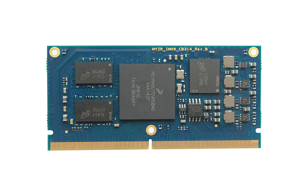
MYZR-I.MX6-CB314-6U7C
1пЉЪDual Core/Industrial Grade
2пЉЪARM Cortex-A9
3пЉЪDDR31GB, up to 2GB
4пЉЪeMMC 4GB, up to 64GB
5пЉЪ-40°C to 85°C
product detailпЉЪ
Front view

Size

MY-IMX6-CB314 parameter
Hardware configuration
| Cord board model | CPU | Memory | Storage | Boot mode | Burning mode | Others |
|---|---|---|---|---|---|---|
| MY-IMX6-CB200 | i.MX 6QP | 1G / 2G | eMMC: 4G ~ 64G | SPI Flash | 2 bit dialing) | Standard configurationпЉЪmemory 1GпЉМstorage 4G |
| i.MX 6Q | 1G / 2G | eMMC: 4G ~ 64G | SPI Flash | 2 bit dialing | Standard configurationпЉЪmemory 1GпЉМstorage 4G) | |
| i.MX 6U | 1G | eMMC: 4G ~ 64G | SPI Flash | 2 bit dialing | Standard configurationпЉЪmemory 1GпЉМstorage 4G | |
| i.MX 6S | 512M / 1G | eMMC: 4G ~ 64G | SPI Flash | 2 bit dialing | Standard configurationпЉЪmemory 512MпЉМstorage 4G | |
| MY-IMX6-CB314 | i.MX 6QP | 1G / 2G | eMMC: 4G ~ 64G | SPI Flash | 2 bit dialing | Standard configurationпЉЪmemory 1GпЉМstorage 4G |
| i.MX 6Q | 1G / 2G | eMMC: 4G ~ 64G | SPI Flash | 2 bit dialing | Standard configurationпЉЪmemory 1GпЉМstorage 4G | |
| i.MX 6U | 1G | eMMC: 4G ~ 64G | SPI Flash | 2 bit dialing | Standard configurationпЉЪmemory 1GпЉМstorage 4G | |
| MY-IMX6-CB336 | i.MX 6QP | 1G / 2G | eMMC: 4G ~ 64G | SPI Flash | 2 bit dialing | Standard configurationпЉЪmemory 1GпЉМstorage 4G |
| i.MX 6Q | 1G / 2G | eMMC: 4G ~ 64G | SPI Flash | 2 bit dialing | Standard configurationпЉЪmemory 1GпЉМstorage 4G | |
| InstructionпЉЪthe series of core boards mentioned above can be offered in grades of automotive/industrial /commercial гАВstandard configuration is commercial grade | ||||||
Temperature range
Working temperature
-
Commercial expansion gradeпЉЪ
-
-
-20°C ~ 85°C
-
-
Industrial gradeпЉЪ
-
-
-40°C ~ 85°C
-
-
Automotive gradeпЉЪ
-
-
-40°C ~ 100°C
-
Storage temperature
-
-
-60°C ~ 125°C
-
Model command rule

Model example
-
MY-IMX6-CB314-6Q5E-1G-4G
-
CPUпЉЪMCIMX6Q5E
-
Memory SizeпЉЪ1G
-
eMMC SizeпЉЪ4G
Operating system support
| Operating system & version) | MY-IMX6-EK200 | MY-IMX6-EK314 | MY-IMX6-EK336 | MY-IMX6-EK140 | |
|---|---|---|---|---|---|
| Linux | Linux-3.0.35 | YES | YES | - | - |
| Linux-3.14.52 | YES | YES | - | - | |
| Linux-4.1.15 | YES | YES | YES | YES | |
| Android | Android 4.2.2 | YES | - | - | - |
| Android 4.4.2 | YES | YES | - | - | |
| Android-5.1.1 | YES | YES | YES | - | |
| QT | QT-4.8.5 | YES | YES | - | YES |
| QT-5.5.0 | YES | YES | YES | - | |
| Ubuntu | Ubuntu 11.10 | YES | YES | - | - |
| Ubuntu 12.04 | YES | YES | - | - | |
Hardware interface
| Display module | HDMI | 1 way | 1.4 port |
| LVDS | 2 way | 8bit mode, up to 165 Mpixels/s | |
| RGB | 1 way | 24 bit mode | |
| Camera | CSI | 1 way | 8 bit mode |
| Mipi | 1 way | 2 Lanes | |
| Ethernet | RGMII | 1 way | 1000M |
| Audio | I2S/SSI/AC97 | 1 way | up to 1.4 Mbps |
| PCI Express | PCI Express | 1 way | Gen 2.0 |
| Storage | SD/MMC card | 2 way | 4/8bit |
| SATA | 1 way | SATA II, 3.0 Gbps | |
| USB | USBOTG | 1 way | 480M high speed |
| USBHOST | 1 way | 480M high speed | |
| CSPI | CSPI | 2 way | High speed |
| UART | UART | 5 way | up to 4.0 Mbps |
| CAN | CAN | 2 way | 1 Mbps each |
| PWM | PWM | 1 way | Configuration of 4 way is optional |
| I2C | I2C | 3 way | supporting 400 kbps |
| IO expansion | Multiple way | 21 way | Can configure without pin |
| Watchdog | Watchdog | 1 way | Hardware watchdog |
| Bus | EIM | 1 way | 16 bit bus expansion |
| Debug | JTAG | 1 way | JTAG debug |
Power Supply
5V input
Defaulted display selection
LVDS0
LVDS0 7-inch TFT crystal liquid displayпЉИ24bit LVDS portпЉЙ
Resolution 1024X600@60Hz
White backlight
Capacitor touch
LVDS1
LVDS1 7-inch TFT crystal liquid displayпЉИ24bit LVDS portпЉЙ
Resolution 1024X600@60Hz
White backlight
Capacitor touch
RGB
LVDS1 7-inch TFT crystal liquid displayпЉИ24bit RGB portпЉЙ
Resolution 800X480@60Hz
White backlight
Capacitor touch
HDMI
HDMI-output пЉИ24bit HDMI portпЉЙ
1920X1080@60Hz, compatible 16/18/24bpp
Definition of pin
| No. | Pin name | Voltag) | No. | Pin name | Voltage |
|---|---|---|---|---|---|
| P1 | GND | 0V | S1 | GND | 0V |
| P2 | GND | 0V | S2 | GND | 0V |
| P3 | GND | 0V | S3 | CSI0_PIXCLK | 2.5V |
| P4 | UART1_RX | 2.5V | S4 | CSI0_VSYNCH | 2.5V |
| P5 | UART1_TX | 2.5V | S5 | CSI0_DAT12 | 2.5V |
| P6 | AUD3_TXC | 2.5V | S6 | CSI0_DAT13 | 2.5V |
| P7 | AUD3_TXD | 2.5V | S7 | CSI0_DAT19 | 2.5V |
| P8 | GPIO_0_CLKO | 3.3V | S8 | CSI0_DATA_EN | 2.5V |
| P9 | AUD3_RXD | 2.5V | S9 | CSI0_DAT17 | 2.5V |
| P10 | AUD3_TXFS | 2.5V | S10 | CSI0_DAT16 | 2.5V |
| P11 | UART5_RXD | 3.3V | S11 | CSI0_DAT14 | 2.5V |
| P12 | UART5_TXD | 3.3V | S12 | CSI0_DAT18 | 2.5V |
| P13 | GND | 0V | S13 | CSI0_DAT15 | 2.5V |
| P14 | GND | 0V | S14 | CSI0_HSYNCH | 2.5V |
| P15 | LVDSO_TX1_N | 2.5V | S15 | GND | 0V |
| P16 | LVDSO_TX1_P | 2.5V | S16 | GND | 0V |
| P17 | GND | 0V | S17 | CAN1_TX | 3.3V |
| P18 | LVDSO_TX2_N | 2.5V | S18 | CAN1_RX | 3.3V |
| P19 | LVDSO_TX2_P | 2.5V | S19 | GND | 0V |
| P20 | GND | 0V | S20 | I2C2_SDA | 3.3V |
| P21 | LVDSO_TX0_N | 2.5V | S21 | I2C2_SCL | 3.3V |
| P22 | LVDSO_TX0_P | 2.5V | S22 | GND | 0V |
| P23 | GND | 0V | S23 | I2C3_SDA | 3.3V |
| P24 | LVDSO_TX3_N | 2.5V | S24 | I2C3_SCL | 3.3V |
| P25 | LVDSO_TX3_P | 2.5V | S25 | GND | 0V |
| P26 | GND | 0V | S26 | UART4_RXD | 3.3V |
| P27 | LVDSO_CLK_N | 2.5V | S27 | UART4_TXD | 3.3V |
| P28 | LVDSO_CLK_P | 2.5V | S28 | GND | 0V |
| P29 | GND | 0V | S29 | CAN2_TX | 3.3V |
| P30 | DISP0_DAT18 | 3.3V | S30 | CAN2_RX | 3.3V |
| P31 | DISP0_DAT22 | 3.3V | S31 | GND | 0V |
| P32 | DISP0_DAT14 | 3.3V | S32 | KEY_COL2 | 3.3V |
| P33 | DISP0_DAT17 | 3.3V | S33 | GND | 0V |
| P34 | DISP0_DAT9 | 3.3V | S34 | LVDS1_TX1_P | 2.5V |
| P35 | DISP0_DAT12 | 3.3V | S35 | LVDS1_TX1_N | 2.5V |
| P36 | DISP0_DAT5 | 3.3V | S36 |